 Quick Navigation
 All projects
  Hardware
 Links
Links Top projects
Alan numitron clock
Clapclap 2313/1386
SNES Pi Webserver
USB Volume/USB toys
Smokey amp
Laser cutter
WordClock
ardReveil v3
SNES Arcade cabinet
Game boy projects
cameleon
Home Presence Detector
 GitHub
AlanFromJapan
 Contact me
 Who's Alan?
Akizukidenshi
Elec-lab
Rand Nerd Tut
EEVblog
SpritesMods
AvrFreaks
Gameboy Dev
FLOZz' blog
Switch-science
Sparkfun
Suzusho
Datasheet Lib
Reddit Elec
Ermicro
Carnet du maker (fr)
Gameboy homebrew cartridge
Last update: Tue Feb 17 20:52:02 2026
Introduction
This is a Gameboy original cartridge with a flash memory store homebrew games. I have no idea is you can put ROMs of commercial games on and I have no interrest in finding out. This is to be used by your unique creations, well, mine in fact :)There will be multiple versions of that board, will be created in that order:
- The modest × Mixed results: just holds the flash and a microcontroller used to upload the flash without a special programmer (which I don't have anyway)
- The revenge working (with a few airwire): just took what I found on the net and mess-up a few things
- The victory working on GBC but not DMG/Pocket: basically mending my hurt pride.
- The ULTIMA working on GBC and DMG/Pocket + multi-ROM: THE ONE TO RULE THEM ALL.
- The DeLuxe (future plan): this time the mCU will sometime steal the spotlights and answer to the GB instead of the flash. Mainly idea is to use the mCU to read a RTC and return time, that's all: making your Gameboy clock.
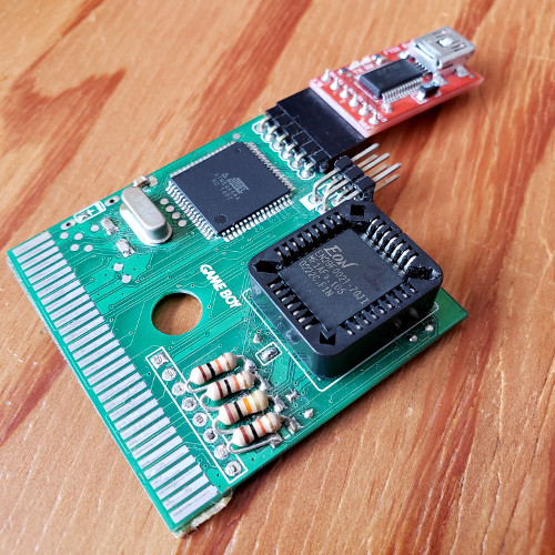
Ultima version - June 2020
Euh ... why? Seriously. You are fixating.
Yeah well, I want to make one board that works fine. And a gentleman on gbdev forums suggested that I add a switch to hold multiple game at once, and I find the idea splendid! So let's do it: take the Victory, fix the bug and add that switch!Fast forward a few weeks: and this works just fine ! 😄😄😄
→ The Eagle code is here on GitHub (pick the "ULTIMA" one)
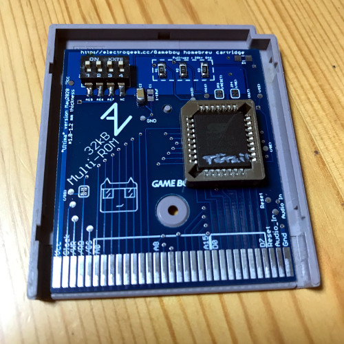
Use as a simple 32kB ROM cartridge
Use as a MULTIPLE (x8) 32kB ROM cartridge
Victory version - May 2020
It works, with 1 airwire as a 32kB cartridge. I redid everything from scratch on this one and did hand routing (a great activity I recommend for passing time, it's like Tetris), but still have 1 issue I didn't forecast.Euh ... why? Seriously.
Because the Revenge below is "ok" (well, it can be made to work) but I made a few mistakes I'd like to fix, to make a """prefect""" cartridge (for me). Ironically this version is not perfect yet but getting closer.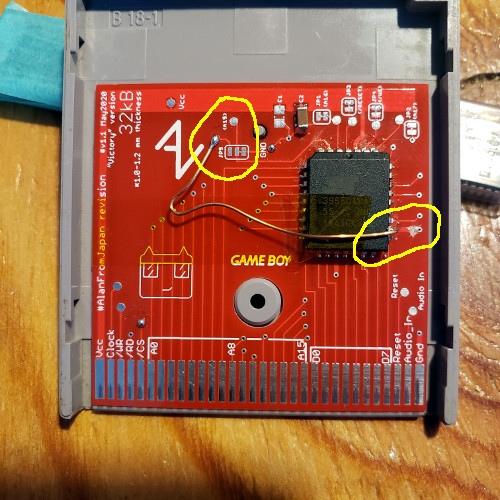
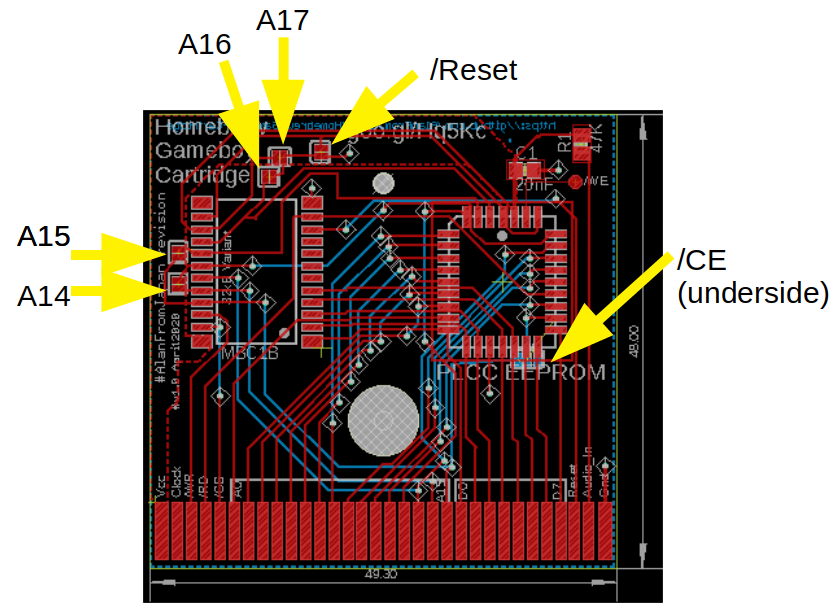
How it's wired (cartridge -> EEPROM):
| Cartridge | EEPROM | Comment |
| A0-A14 | A0-A14 | |
| A15 | GND | EEPROM is tied to GND, but can be connected to cartridge via solderbridge WRONG! Cartridge A15 must be connected to /CE (pin 22) of the EEPROM |
| A16-A17 | Both tied to GND | |
| D0-D7 | D0-D7 | |
| Clock | unused | |
| /WR | VCC | EEPROM is tied to VCC, but can be connected to cartridge via solderbridge |
| /RD | /OE | |
| /CS | GND | EEPROM is tied to GND (always enabled) |
| Reset | VCC | EEPROM is tied to VCC, but can be connected to cartridge via solderbridge |
| Audio in | Ignored (no 47kOhm resistor but can be airwired) | |
| VCC | VCC | |
| GND | GND |
Revenge version - April 2020
It works, with a few airwires or solder-blobs, as a 32kB cartridge. This is based on that gentleman work, credits go to him (though I think he might have some of the same issues).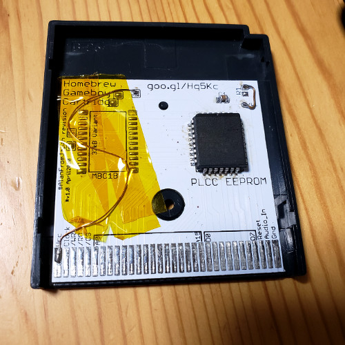
Euh ... why?
5 years ago (now 2020Q2) I made the modest and it failed. Tried again, and it DOES work (see below for details). However you can't read a game with it in a GameBoy. So I found on the net the below versions that look simple enough that I can "inspire" (read "rip off") and make the same. Will cost me about the same but if it works I'll have 10 cards and not 1. And if it still fails, I'll have learned a few things.So I decided to not reinvent the wheel: indeed I found this (its 32kB version), which I thought I could use a base until I found I would do no major change... so since I couldn't send to production someone else's job without messing it up, I spend a few hours moving things around, fixing what I thought needed to be fixed, and there, sent to production.
Everything is on my fork of his project, in the "32kB-variant" branch.
Verdict?
|
It works v(^_^)v but there's a few issues:
From that point I consider you just use the EEPROM in PLCC32 format: That's a bit ugly but it works now. Enjoy! |
 |
Improvements
Modest version (a PLCC32 EEPROM programmer)
This is a half-success/half-failure: it does not work as a GB cartridge (it might, but the form factor is failed so can't even plug it), but it does work fine as an PLCC32 EEPROM programmer! Use this program to drive it from your PC read/write EEPROMs. No real time answering instead of the flash memory: just program or even skip the mCU entirely and just put the flash.
Parts
- ATmega64a because I need a small foot print and lots of pins (18 address, 8 data, 4 control...) http://akizukidenshi.com/catalog/g/gI-04255/
- EN29F002T: 2Mbit flash memory, very cheap http://akizukidenshi.com/catalog/g/gI-01459/
- 16MHz crystal, max for this mCU
- A few pullups resistors and caps
Schematics
See on my Github.README:
- Gameboy game port expects a 2-2.1mm thick board so
- do that PCB 2mm thick, or
- do it 0.6mm and you stick it in a existing cartridge or
- (my current option) you make board 1mm thick, cut out the connector part of a spare board and glue/doubleface tape them: your connector part will be 2mm which should make your GB happy
- Card was mostly autorouted with very thin signals 0.1524 wires. It works but signals are easily damaged by a hot iron or a careless tinkerer. Be careful.
- Autorouted 'cause I'm lazy, but result is ok (at least it works)
- I should stop trying putting a gnd mask everywhere, it's a risk with such thin wires
- Stop using too small font: all the 0.6 font were just not printed, resulting in a blank pcb
- Next time don't put wires below the insertion pads, friction will kill them (one day)
- Next time have an option to just solder the flash, not use the socket: it's too thick and don't fit in a GB
- Could have done that with a smaller 88a for instance, with a SIPO to address the need of pins (cheaper, easier to source, and less waste of power)
Code
 On my GitHub.
Fuses
ATmega64a are tricky little b*stards and letting a fuse set cost me 2 weeks of time.You must unset JTAGEN (or pins PF4-PF8 won't be generic I/O) and unset CompMode. For the clock I picked EXTHIFXTALRES_1KCK_0MS: I run the mCU with a 16MHz crystal, the max speed for this model.
Here's what you should set:
- Extended: 0xFF
- High: 0xD9
- Low: 0xEE
Documentation
- Just buy it: a long list of available cartridge https://gr33nonline.wordpress.com/2019/03/21/gameboy-flashers/
- https://www.gamasutra.com/blogs/DoctorLudos/20171207/311143/Making_a_Game_Boy_game_in_2017_A_quotSheep_It_Upquot_PostMortem_part_12.php
- https://dhole.github.io/post/gameboy_cartridge_emu_1/
- https://reinerziegler.de.mirrors.gg8.se/readplus.htm
- Very good tutorial en francais about how to program a GB software using wla http://furrtek.free.fr/?a=gbasm
- The toolchain is here http://www.villehelin.com/wla.html
- Another option is using GBDK http://sourceforge.net/projects/gbdk/
- The emulators are bgb or no$gba ("no cash gba")
- Make my own cartridge
- Use this ROM ? 2MBits x2 for 250 jpy http://akizukidenshi.com/catalog/g/gI-01459/
- And one gentleman who used it https://github.com/kshoji/FlashWriter/blob/master/Arduino/FlashROMWriter.ino
Things I'd like to copy:
Good tutorial on the card making and z80 http://www.digital-circuitry.com/8-bit_Memory_Mapping.htm
Internal
- Gameboy screen has details about the technicalities around the gameboy screen (hardware wise)
- Gameboy guts and programming in case I change my mind and just make a custom cartridge.
External
- Holly Grail "Pan docs" http://gbdev.gg8.se/wiki/articles/Main_Page
- Memory bank explained http://gbdev.gg8.se/wiki/articles/Memory_Bank_Controllers
- Gameboy Pandocs http://problemkaputt.de/pandocs.htm
- http://dhole.github.io/post/gameboy_cartridge_emu_1/
- Hackaday category http://hackaday.com/category/nintendo-gameboy-hacks
- https://www.insidegadgets.com/2011/04/23/emulating-the-nintendo-logo-on-the-gameboy/


electrogeek.tokyo ~ Formerly known as Kalshagar.wikispaces.com and electrogeek.cc (AlanFromJapan [2009 - 2026])